-
Notifications
You must be signed in to change notification settings - Fork 17
Introduction to Verilog

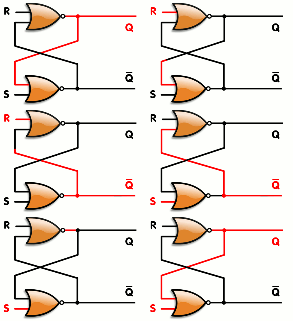
[source: http://en.wikipedia.org/wiki/File:R-S_mk2.gif]
Hardware
Description
Language
We use Verilog to describe hardware
(Other languages exist, such as VHDL. CAUTION: arguing about which language is better will result in expulsion from the room for 10 minutes. Schematic entry exists but rarely used by experienced designers.)
Wires connect logic elements.
Wires have no memory.
Wire 'state' is determined by what 'drives' them.
In reality, wires will have a state of 1 or 0.
In simulation, wires could have a state of X (unknown), which often means that the driver of the wire hasn't been initialised.
Elementary single bit memory unit
(Latches are considered harmful)

[source: http://breadboardgremlins.files.wordpress.com/2013/01/logic-cell.png]
Elementary logic unit
"Large" memory blocks

[source: https://i.imgflip.com/90aot.jpg]
That there is no main()?!
Everything runs concurrently
Think left to right, not top to bottom
`define ROUNDS 4 // global constants
parameter param1=<value>; // local parameters
reg  [nn:mm] foo, bar;
wire [nn:mm] oof, rab;
Creating a module:
module <module_name> (
  // declare ports
  input  [nn:mm] <port_name_1>,
  output [nn:mm] <port_name_2>
  ...
);
  // instantiate registers
  // name wires
  ...

  // logic goes here
  ...

endmodule
or
module (<port_name_1>, <port_name_2> ...);

  input  [nn:mm] <port_name_1>;
  output [nn:mm] <port_name_2>;

  ...

endmodule
<module_name> <unique_instance_name> (.<port_name_1>(<wire_name_1>),
                                      .<port_name_2>(<wire_name_2>));
`define ROUNDS 32
a = `ROUNDS;
b = a / 4;

b = a;
c = b;
What is the value of b and c?
b <= a;
c <= b;
What is the value of b and c?
Always use non-blocking assignments! (unless they're in a testbench and you need a sequence of operations)
Think in bits!
In an FPGA every memory bit (register, flip-flop) is at a state of either 0 or 1
Values can be expressed in several ways:
a <= 10; // decimal
b <= 4'b1010; // binary
c <= 4'd10; // decimal
d <= 4'hA; // hex
e <= {2'b10, 2'b10};
f <= {1'b1, 1'b0, 1'b1, 1'b0};
all represent the same bit sequence.
g <= ~4'h5;
h <= 4'hE & 4'b1011;
i <= 4'd9 | 4'h3;
j <= 4'b0101 ^ 4'b1111;
all result in the same bit sequence.
reg [03:00] temp, result;

temp <= 4'd9 + 4'd7;
result <= temp & 4'h3;
What is the value of result?
In simulation you'll get a value of X ('undetermined') if no initial value has been set. Again, in the FPGA it will be either a 0 or 1.
FPGA code is almost always synchronous, which means that events happen on clock edges. The rest of the time, signals propagate through the device and through logic.
Always think about the clock; nothing happens without it.
Since everything runs all the time, we use 'states' to determine when to evaluate an input signal and when to change an output. All but the very basic HDL code has 'finite state machines' that control the behaviour of the design.

[source: http://en.wikipedia.org/wiki/File:Turnstile_state_machine_colored.svg]
module turnstile (
  input CLOCK,
  input PUSH,
  input COIN,
  input RESET,
  output UNLOCKED
);

reg state, nextstate;

assign UNLOCKED = state;

parameter LOCKED_STATE=1'b0, UNLOCKED_STATE = 1'b1;

always @(posedge CLOCK) begin
  if (!RESET) state <= next_state;
  else state <= LOCKED_STATE;
end

always @(posedge CLOCK) begin
  if (RESET)
    next_state <= LOCKED_STATE;
  else
    case (state)

      LOCKED_STATE:
      begin
        if (coin == 1'b1)
          next_state <= UNLOCKED_STATE;
      end

      UNLOCKED_STATE:
      begin
        if (push == 1'b1)
           next_state <= LOCKED_STATE;
      end

      default:
      begin
        // ALWAYS have a default for a case statement,
        // even if all possible cases are covered
        next_state <= LOCKED;
      end
  endcase
end
* this snippet is a good start, but more is needed for a robust design
Finite state machines can have many, quite complicated, states, so it's good practice to draw a state diagram on paper before starting to code! A concise intro to FSMs in Verilog is here.
Ask yourself
- Is it working in simulation?
- Is the clock working and reaching the logic?
- Is my logic still there?
Don't freak out if you get a gazillion warnings; it's perfectly normal in this world of FPGA tools!
Other than searching for the error message, http://electronics.stackexchange.com or http://stackoverflow.com are good places to find answers and ask questions. A concise, but comprehensive, guide to Verilog can be found here: http://www.doe.carleton.ca/~jknight/97.478/PetervrlK.pdf
Create a lower frequency clock from the main 50 MHz clock and output a pattern on the LEDs
Create a single pulse of a particular clock period from an incoming pushbutton signal
Edge detect circuit:

Output a Fibonacci number update on the LEDs (in binary) whenever KEY1 is pressed. Reset the pattern when KEY0 is pressed. When the Fibonacci number exceeds what can be displayed on the LEDs, display a unique pattern (such as blinking all LEDs multiple times) on the LEDs, then reset.
Example state diagram (can be done differently and more efficiently):

Using the switches, LEDs and pushbuttons, implement a 4-bit 4-gidit lock. Each combination digit is entered using the switches and a press of KEY1. A pattern should let the user know whether the combination succeeded or failed. (Watch out for insecure implementations!) Extra credit for locking the interface after three wrong attempts. Super extra credit for allowing the user to re-set the initial combination after a successful entry.
Hints:
- Start by connecting each switch to an LED and see if it turns on/off when the switch is moved positions
- Create a state diagram on paper before starting to coding
- An example design can be found in the repo; use it if you're stuck, or as a starting point
Create a 4-bit arithmetic logic unit (ALU) using the LEDs, pushbutton and switches. The ALU should support addition, subtraction, multiplication, and division of 4-bit numbers. Use the switches and pushbuttons as for digit and arithmetic operation choice. Use the LEDs for displaying status and results.
Choose a DE0-nano peripheral of your choice and write a driver for it. UART may be simplest (implement transmit first), though implementing basic I2C and SPI functionality is also doable. Be creative!
A UART (Universal Asynchronous Receiver/Transmitter) is a common serial communications interface found in chips. Usually, 2 physical connections are made between the receiver and transmitter, with each wire used for communications in a single direction. It works by both ends operating with a common rate of transmission and using a very basic protocol. At a digital level, it is a relatively simple block to design, and typically most of the design effort is around making it configurable, and interfacing it with the rest of the system.
In this exercise we will design the fundamentals of a UART transmit (TX) block and make it transmit some characters to a listening PC.
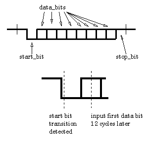
UART communication is typically byte based and uses a very simple protocol on a single wire. Each byte is sent individually serially, beginning with a start bit and finishing with an end or stop bit. The receiving end synchronises to the start bit, samples (measures) the line at periods when it's known to be stable (this is why a rate of transmission must by known) and re-assembles the bits into a byte.
It couldn't be simpler than that! So 10 bits for every 8-bit byte transmitted. The start bit is 0 and the end bit is 1.
The UART line is logically high when it is idle. This is why the start bit is 0 so the receiver can sample for this falling edge, and based on the transmission rate, know when to sample the middle of each bit period.
The data is transmitted least significant bit first.
The major parts of a UART transmitter are
- a state machine to organise when the start, data bits and stop bits are represented on the line
- a clock division (counting) scheme to determine when to change the output bit when transmitting
The baud rate (bit rate) we'll use in 115200. That's a transmission rate of 115200 bits a second.
The board's 50MHz clock must be divided down to this rate to drive the transmit logic.
Build a system which takes the 50MHz clock and generates a 115.2kHz clock.
Use this to run a state machine which
- starts off by transmitting the data 0x30 (ASCII '0') after reset
- then detects if the pushbutton 1 (Key 1) has been pressed, and if so
- increment the data by 1
- retransmits this new data
- Once the data reaches the value 0x7a, the next value should again be 0x30
A majority of the design has been provided. You will have to:
- Determine the number at which the clock divider should wrap
- Finish the state machine to control the states transmitting the start, 8 data, and stop bits.
A testbench is provided in uart_tb.v, which will decode the the UART transmission, and finish when it detects a successful transmission of the entire sequence from 0x30, to 0x7a and back to 0x30.
For Linux:
To run the testbench, simply type:
make run
If successful you will see the decoded UART transmit for each character stream out.
View the output with GTKWave with
gtkwave waves.vcd
For Windows:
Please load the uart.v and uart_tb.v into a Quartus project and simulate using the usual methods.
For Linux:
In the uart/ directory, a uart.tcl file and Makefile will allow you to build and program the FPGA from the command line with
make pgm
For Windows:
Please configure the design using the Quartus IDE.
The uart.qpf and uart.qsf files may of some value to indicate the pins mappings.
Getting UART output back to your PC requires 2 steps:
- Making the physical connection between the board and the PC
- Getting the PC software to read the UART input
Attaching the Embecosm UART module to the board is done by attaching it so the DTR pin is on pin 37 of the JP2 (GPIO-1) header. See this guide for a pinout diagram

Then attach the UART board to the PC via a USB cable.
Linux:
We can monitor the UART by running the screen tool. We will assume the UART device has appeared in the system's /dev directory as /dev/ttyUSB0. We will use the buad rate (as already mentioned) of 115200.
screen /dev/ttyUSB0 115200
If screen exits citing permissions errors, run the following:
sudo chmod a+rwx /dev/ttyUSB0
.. and try launching screen again.
Note: To exit screen once you're done, press: ctrl+a then k and y for yes to Really kill this window [y/n].
Optionally, if you don't have screen installed you can try
cat /dev/ttyUSB0
Windows:
Try connecting to the board via putty.
Press KEY1 to make the UART transmit the next chracter. You should see it turn up on the UART console, and see the LEDs increment showing the value last transmitted.


